 It’s our pleasure to announce that HacDC is now the proud owner of a scanning electron microscope (SEM)! An SEM is a scientific instrument capable of producing extremely high-magnification images: magnifications of 5,000x to 500,000x are routinely achieved by these machines. Additionally, SEMs can be interfaced with additional detectors to examine the atomic composition and other characteristics of both organic and inorganic samples. These makes them extremely useful machines for imaging, scientific analysis, and even processes such as e-beam lithography.
If you’re unfamiliar with the incredible images that SEMs can produce, check out this gallery.
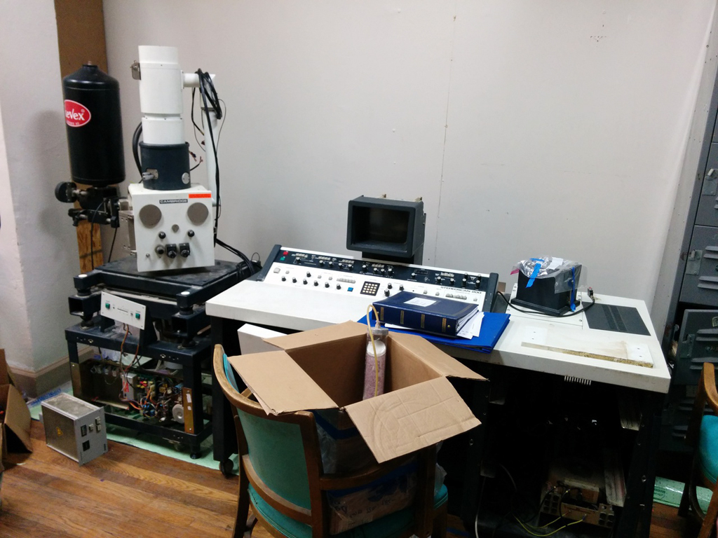
Our machine is an older, second-hand model, and was graciously donated to us by 757 Labs. It’s a Cambridge Stereoscan 200 from 1983. Despite its age, it was widely renowned for being a very versatile machine, and all the electronics are well within the realm of being understandable and repairable by the hobbyists and professionals at the hackerspace. It’s currently undergoing member-driven inspection and repair.
Its current status, as well as information about planned projects, can be found on our wiki.
For the inquiring mind: the theory of operation of a standard SEM is relatively straightforward: a metal specimen chamber and hollow column are pumped down to near-vacuum (between 10e-8 to 10e-11 atmospheres!) via the operation of a roughing pump and a turbomolecular or oil diffusion pump. A power supply then runs current through a tungsten filament to cause thermionic emission of electrons—very similar to the operation of a light bulb. Another power supply creates a voltage relative to a nearby anode, which accelerates the electrons to a high energy, adjustable from 1 to 40 keV (kiloelectronvolts). The electrons spray out from the filament towards the anode, but are gradually reduced down to a very small spot size via a series of electromagnetic lenses and one or more metal apertures. This small spot of electrons finally hits the sample. Additional circuitry deflects the small spot of electrons over the sample’s surface, effectively scanning it across the area to be examined, much like a beam inside of a cathode ray television. At this point secondary and backscattered electrons are kicked out of the sample and detected by a sensor inside the chamber, which passes the signal along to processing circuitry, ultimately resulting in an image being displayed on a TV.
If you’re as excited as we are by these images and would like to make your own, or if you’d like to learn more about the nitty-gritty details above, you’re probably the sort of person we’re looking for! We’d love to find members who would like to assist with the repair and operation of the machine, as well as planning future improvements.
(Written by: Dan K and Phil S)