 DIY printed circuit boards (PCB) are an intermediate step toward mass producing an industrial-grade integrated circuit.
After prototyping a project using tools like a solderless breadboard, small-run or one-off PCBs are a good choice when you want a more structurally stable version of your circuit that is destined for mass production. Perhaps you would like to be able to install it into a larger project prototype. Once all the what-ifs and tests are successful with these hand-made PCBs, higher resolution industrial processes can be used to fabricate more robust PCBs.
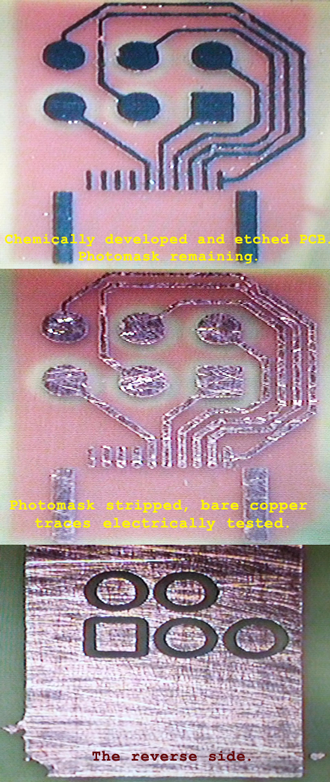
Thanks to members, mirage335 and Dan Barlow, we now have a standardized method to fabricate DIY PCBs with traces (conducting areas) and spacing (non-conductive areas) of 6 mil (0.15mm).
For projects where the 10 mil tolerances made possible by our CNC mill are not enough, photolithography is a good alternative. The process uses light-sensitive coatings to mask conductive surfaces before etching. The result is a a lovely printed circuit where before you had a jumble of wires. The process, workflow, and references are described by mirage335 on our wiki.
Interested in this topic? Check our events calendar and visit us! Want to see lots more like it? Support us!